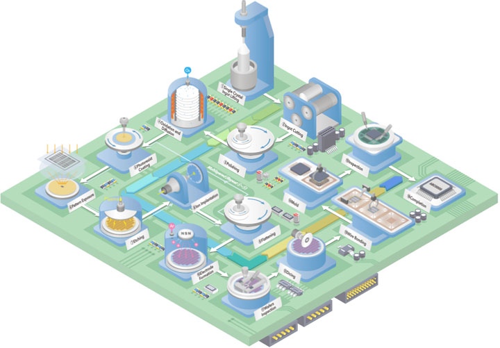
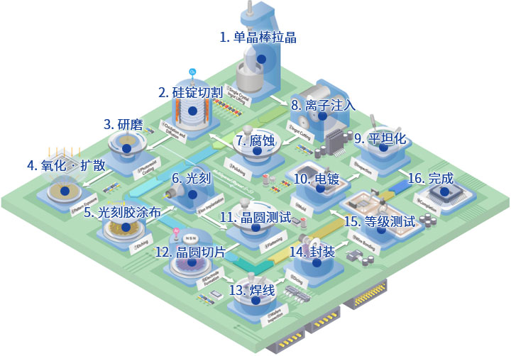
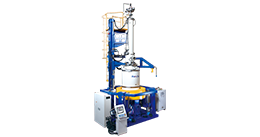
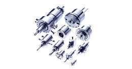
Single Crystal Ingot pulling
The process of slowly rotating and pulling the dissolved polysilicon material to make a single crystal ingot.
Oxidation • diffusion
Film formation on the surface of silicon wafer.
Photoresist coating
The photoresist is uniformly coated on the surface of the wafer and its properties change when exposed to ultraviolet light.
Lithography
The photoresist layer is exposed to ultraviolet light through a mask to form an electro pattern.
Corrosion
Remove any unwanted photoresist with a plasma etcher.
PECVD
Ions are injected into the acidified film to form a semiconductor with desired properties. And, to multilayer, make an insulating film.
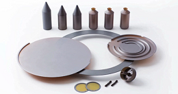
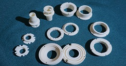
Grinding
The silicon wafer is ground into a mirror shape.
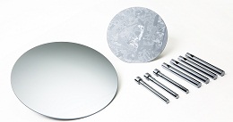
Silicon ingots
Slice monocrystalline silicon ingot horizontally with diamond wire saw.
Grade test
Identify key features of each processor, such as maximum power, power consumption, and heat generation.
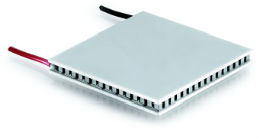
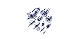
Encapsulation
The substrate, the core, and the heat sink are stacked together to form a processor. Finally, remove from the fixed plate.
flattened
Polish the wafer surface.
Electroplating
Electroplate a layer of copper sulfate to precipitate copper ions onto the transistor. After electroplating, a thin layer of copper is formed.
Wafer test
Each chip fabricated on the wafer is functionally tested with a defective portion.
Wafer slicing
Cut a wafer into pieces, each of which is a processor core.
Welding wire
Secure the processor with the fixed plate and weld the wire.
Complete
Print the product model.